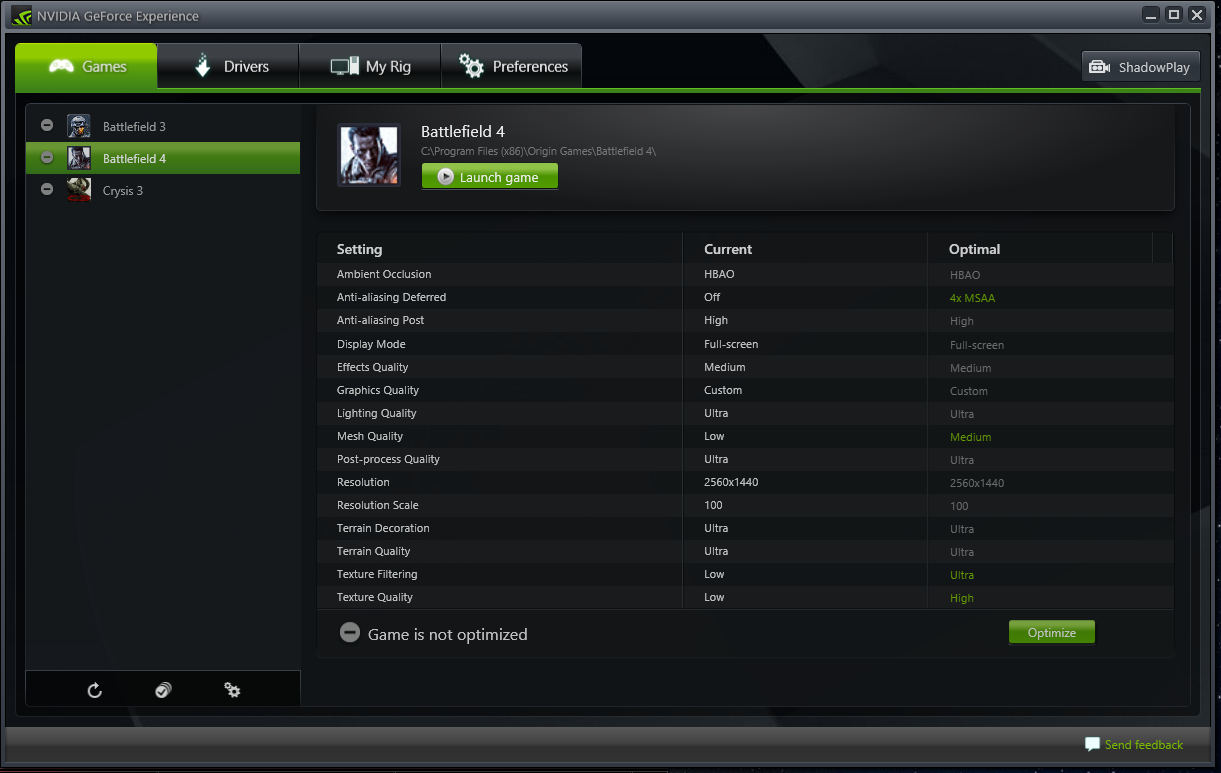
Last night I sold my GTX 770 and upgraded to the GTX 780. The recent price drops helped my decision. That and the performance gains, which can be summed up nicely by the GeForce Experience settings. The screen shot below shows the before (Current) and after (Optimized) setting. I should stay around 60 FPS in the below game (Battlefield 4), but I will gain back the anti-aliasing, some texture details, and some mesh detail that I had lost when making the jump from Battlefield 3 to 4 (Battlefield 4 being a much more graphically demanding game).
The 780 uses the same “Kepler” architecture as the 770, but basically doubles the die size to 7.1B transistors (vs. 3.5B on the 770). The 780 also adds 1GB of VRAM bringing the total to 3GB. The extra kick of VRAM is likely where the anti-aliasing performance comes from. And the doubling of die size is what’s giving us the raw horse power to gain back the texture/mesh details.
History Lesson -> About 2 years ago now Nvidia released the GTX 680. This was the first card built on the Kepler architecture and, like the 770, had a die size of 3.5B transistors. The 680 was rated with a 195W TDP and preformed great at the time. Fast forward 1 year to the summer of 2013, and it was time for Nvidia’s yearly product refresh. With no new architecture until 2014, the solution was to put the 680 on steroids. Same die size, faster clocks – hence the 770’s new TDP of 230W. This move however, would not be enough to stave off the competition, and more importantly would allow that competition to overtake Nvidia’s “fastest GPU” crown. So with the 770 now slotting into Nvidia’s #2 position, the new #1 would need to gain performance. To do this Nvidia doubled the 770’s die size, gaining performance in numbers. Interestingly enough, despite the 780’s larger foot print, both the 770 and 780 consumer roughly the same amount of power (~250W). Gaining performance in numbers rather than by clock speed increases proves to be more efficient.

